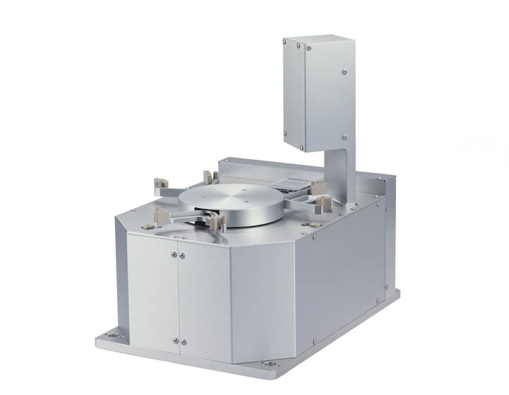
MAF-HJ
This 200mm mechanically clamping wafer aligner minimizes wafer particle contamination by avoiding contact with the backside of the wafer.


Features
- Clean alignment enabled by limiting contact to the wafer edge.
- Notch/Flat are automatically recognized, eliminating the need for host controller settings.
- Buil-in controller for a compact design.
Specifications
| Handling object |
φ200mm SEMI/JEIDA standard wafer. |
| Alignment time |
9.0seconds or less (23.0seconds of less when separate chucking required) |
| Alignment accuracy |
θ:±0.2° or less(3σ) |
| Wafer off-center limit |
±1mm or less (Wafer offset from chuck center) |
| Wafer holding method | Edge hold |
| Wafer hold check | Photo micro sensor |
| Communication |
RS-232C(Serial Interface) |
| Utility |
Power:DC24V±10% 3A 1line Dry air:φ6mm 0.35MPa to 0.4MPa 1line |
| Mass | Main body:Appox.8kg |
Contact us for questions about products.